Page 2 - YMF724F; LOGOS; of virtual acoustic sound to the XG format.; and indicates GM system level 1 Compliant.
YMF724F September 21, 1998 -2- LOGOS 1. GM system level 1 GM system level 1 is a world standard format about MIDI synthesizer which provides voice arrangements and MIDI functions. 2. XG XG is a format about MIDI synthesizer that is proposed by YAMAHA, and keeps the upper compatibility of GM system l...
Page 3 - PIN CONFIGURATION; 44 Pin LQFP Top View
YMF724F September 21, 1998 -3- PIN CONFIGURATION YMF724F-V GP4GP5GP6GP7RXDTXD ROMDO/VOLDW#ROMSK/VOLUP# VDD5VDD3 VSSVSS IRQ5IRQ7IRQ9 IRQ10IRQ11INTA# VSS RST#VDD5PVSS PCICLK GNT#REQ#AD31AD30AD29PVSSAD28AD27AD26PVSSAD25AD24 1 23456789 101112131415161718192021222324252627282930313233343536 1081071061051...
Page 4 - PIN DESCRIPTION
YMF724F September 21, 1998 -4- PIN DESCRIPTION 1. PCI Bus Interface (53-pin) name I/O Type Size function PCICLK I P PCI Clock RST# I P Reset AD[31:0] IO Ptr Address / Data C/BE[3:0]# IO Ptr Command / Byte Enable PAR IO Ptr Parity FRAME# IO Pstr Frame IRDY# IO Pstr Initiator Ready TRDY# IO Pstr Targe...
Page 6 - TYPE
YMF724F September 21, 1998 -6- 6. Miscellaneous (15-pin) name I/O type Size function ROMCS O T 3mA Chip select for external EEPROM ROMSK / VOLUP# IO Tup 3mA Serial clock for external EEPROM or Hardware Volume (Up) ROMDO / VOLDW# IO Tup 3mA Serial data output for external EEPROM or Hardware Volume (D...
Page 7 - BLOCK DIAGRAM
YMF724F September 21, 1998 -7- BLOCK DIAGRAM PCI Bus Interface BUS Master DMA Controller Memory XG Synthesizer Direct Sound Acc. Wave In/Out PC-PCI / D-DMA / S-IRQ SB Pro OPL3 MPU401 Joystick Rate Converter / Mixer AC-2 Interface SPDIF (output) AC3F2 Legacy Audio PCI Audio Interface
Page 8 - SYSTEM DIAGRAM; MMSystem
YMF724F September 21, 1998 -8- SYSTEM DIAGRAM WaveIn Device WaveOut Device MidiOut Device XG/DLS Engine DS-1 Slot Manager (Up to 64-sound) Soft Effect DirectSound HAL DLS Appllication AC-3 Application DirectX Application DirectSound VxD YMF724F(DS-1) MMSystem MidiOut Device MidiIn Device DOS VM I/O ...
Page 9 - FUNCTION OVERVIEW
YMF724F September 21, 1998 -9- FUNCTION OVERVIEW 1. PCI INTERFACE DS-1 supports the PCI bus interface and complies to PCI revision 2.1. 1-1. PCI Bus Command DS-1 supports the following PCI Bus commands. 1-1-1. Target Device Mode C/BE[3:0]# Command 0 0 0 0 Interrupt Acknowledge (not support) 0 0 0 1 ...
Page 10 - read from these registers are all zero.
YMF724F September 21, 1998 -10- 1-2. PCI Configuration Register In addition to the Configuration Register defined by PCI Revision 2.1, DS-1 provides proprietary PCI Configuration Registers in order to control legacy audio function, such as OPL3, Sound Blaster Pro, MPU401 and Joystick. These addition...
Page 11 - This bit enables DS-1 to response to Memory Space Access.
YMF724F September 21, 1998 -11- 00 - 01h: Vendor ID Read OnlyDefault: 1073hAccess Bus W idth: 8, 16, 32-bit b15 b14 b13 b12 b11 b10 b9 b8 b7 b6 b5 b4 b3 b2 b1 b0 Vendor ID b[15:0] ........Vendor ID This register contains the YAMAHA Vendor ID registered in Revision 2.1. This register is hardwired to ...
Page 12 - Error on special cycle.
YMF724F September 21, 1998 -12- b8 ................SER: SERR# Enable This bit enables DS-1 to drive SERR#. “0”: Do not drive SERR#. (default) “1”: Drives SERR# when DS-1 detects an Address Parity Error on normal target cycle or a Data Parity Error on special cycle. 06 - 07h: Status Read / W rite Cle...
Page 13 - 9h: Programming Interface; Multimedia Base Class.
YMF724F September 21, 1998 -13- 08h: Revision ID Read OnlyDefault: 03hAccess Bus W idth: 8, 16, 32-bit b7 b6 b5 b4 b3 b2 b1 b0 Revision ID b[7:0] ..........Revision ID This register contains the revision number of DS-1. This register is hardwired to 03h. 09h: Programming Interface Read OnlyDefault: ...
Page 15 - this ID to their Vendor ID in the BIOS POST routine.; in the BIOS POST routine.; 4h: Capability Register Pointer; Configuration register, and this register indicates “50h”.
YMF724F September 21, 1998 -15- 2C-2Dh: Subsystem Vendor ID Read OnlyDefault: 1073hAccess Bus W idth: 8, 16, 32-bit b15 b14 b13 b12 b11 b10 b9 b8 b7 b6 b5 b4 b3 b2 b1 b0 Subsystem Vendor ID b[15:0] ........Subsystem Vendor ID This register contains the Subsystem Vendor ID. In general, this ID is use...
Page 16 - This register is hardwired to 05h.; This register is hardwired to 19h.
YMF724F September 21, 1998 -16- 3Ch: Interrupt Line Read / W riteDefault: 00hAccess Bus W idth: 8, 16, 32-bit b7 b6 b5 b4 b3 b2 b1 b0 Interrupt Line b[7:0] ..........Interrupt Line This register indicates the interrupt channel that INTA# is assigned to. 3Dh: Interrupt Pin Read OnlyDefault: 01hAccess...
Page 19 - MPU401 mode form default to UART, is returned.
YMF724F September 21, 1998 -19- 42 - 43h: Extended Legacy Audio Control Read / W riteDefault: 0000hAccess Bus W idth: 8, 16, 32-bit b15 b14 b13 b12 b11 b10 b9 b8 b7 b6 b5 b4 b3 b2 b1 b0 IMOD SBVER SMOD - - MAIM JSIO MPUIO SBIO FMIO b[1:0] ..........FMIO: FM I/O Address allocation These bits determin...
Page 20 - 4-45h: Subsystem Vendor ID Write Register
YMF724F September 21, 1998 -20- b[12:11] ......SMOD: SB DMA mode These bits determine the protocol to achieve the DMAC(8237) function on the PCI bus. “0”: PC/PCI (default) “1”: reserved “2”: Distributed DMA “3” reserved b[14:13] ......SBVER: SB Version Select These bits set the version of the SB Pro...
Page 22 - includes OPL3 and SB Pro engines.; This bit controls the power state of the ADC and Input Mux in AC-2.
YMF724F September 21, 1998 -22- b2 ................DPLL1: Disable PLL1 Clock Oscillation Setting this bit to “1” disables the oscillation of PLL for the PCI Audio function. “0”: Normal (default) “1”: Disable b3 ................PSL0: Power Save Legacy Audio Block 0 Setting this bit to “1” stops provi...
Page 23 - register without causing an error.; Master; - Set PSL0 and PSL1 bits to “1”, when DPLL0 bit is set to “1”.
YMF724F September 21, 1998 -23- b12 ..............PR4: AC-2 Power down Control 4 This bit controls the power state of the AC-link in AC-2. “0”: Normal (default) “1”: Power down b13 ..............PR5: AC-2 Power down Control 5 Setting this bit to “1” disables the internal clock of AC-2. In case AC-2 ...
Page 24 - This bit enables the Distributed DMA function.
YMF724F September 21, 1998 -24- 4C-4Dh: D-DMA Slave Configuration Read / W riteDefault: 0000hAccess Bus W idth: 8, 16, 32-bit b15 b14 b13 b12 b11 b10 b9 b8 b7 b6 b5 b4 b3 b2 b1 b0 Base Address EA TS CE b0 ................CE: Channel Enable This bit enables the Distributed DMA function. “0”: Disable ...
Page 25 - 1h: Next Item Pointer; The default value is “0”.
YMF724F September 21, 1998 -25- 51h: Next Item Pointer Read OnlyDefault: 00hAccess Bus W idth: 8, 16, 32-bit b7 b6 b5 b4 b3 b2 b1 b0 Next Item Pointer b[7:0] ..........Next Item Pointer DS-1 does not provide other new capability besides Power Management. This register is hardwired to 00h. 52-53h: Po...
Page 26 - When the power state is changed from D3
YMF724F September 21, 1998 -26- 54-55h: Power Management Control / Status Read / W riteDefault: 0000hAccess Bus W idth: 8, 16, 32-bit b15 b14 b13 b12 b11 b10 b9 b8 b7 b6 b5 b4 b3 b2 b1 b0 - - - - - - - - - - - - - - PS b[1:0] ..........PS: Power State These bits determine the power state of DS-1. DS...
Page 27 - ISA Compatible Device; Basically, these registers are configured by the BIOS.
YMF724F September 21, 1998 -27- 2. ISA Compatible Device DS-1 contains the following functions to maintain the compatibility with the past ISA Sound Devices. These devices are considered Legacy devices and the functions are referred to as Legacy Audio. Legacy Audio is independent from PCI Audio and ...
Page 28 - using Intel 430TX chip set is shown below.
YMF724F September 21, 1998 -28- DS-1 supports PC/PCI and D-DMA protocols to emulate the DMA of SB Pro on the PCI. In addition, DS-1 supports the old type of interrupts used by ISA and the Serialized IRQ protocol. Yamaha recommends the combination of PC/PCI and Serialized IRQ. The system block diagra...
Page 32 - SB Pro commands are supported.; CMD Support Function; 0h is always transferred.
YMF724F September 21, 1998 -32- 2-2-1. DSP Command The following shows the list of DSP Commands that are supported by the SB Pro engine. Both SB and SB Pro commands are supported. CMD Support Function 10h o 8bit direct mode single byte digitized sound output 14h o 8bit single-cycle DMA mode digitize...
Page 33 - The conversion for each case is described below.
YMF724F September 21, 1998 -33- 2-2-2. Sound Blaster Pro Mixer The following shows the register map of the Mixer section of Sound Blaster Pro. Address b7 b6 b5 b4 b3 b2 b1 b0 Remark 00h Reset 04h Voice Volume L "1" Voice Volume R "1" 0Ah - - - "1" - MIC Volume* 0Ch - - Ifilte...
Page 35 - from the SCAN DATA register.; This bit stops the internal state of the Sound Blaster block.
YMF724F September 21, 1998 -35- 2-2-3. SB Suspend / Resume The SB block can read the internal state as to support Suspend and Resume functions. The internal state is made up of 218 flip flops. To read the state, these states are shifted in order and read 8 bits at a time from the SCAN DATA register....
Page 36 - This is the data port for reading and writing the internal state.; F8h: Interrupt Flag Register
YMF724F September 21, 1998 -36- F1h: Scan In/ Out Data Read / W riteDefault: 00h b7 b6 b5 b4 b3 b2 b1 b0 SCAN DATA b[7:0] ..........SCAN DATA This is the data port for reading and writing the internal state. F8h: Interrupt Flag Register Read OnlyDefault: 00h b7 b6 b5 b4 b3 b2 b1 b0 - - - - - - - SBI...
Page 38 - DMA Emulation Protocol
YMF724F September 21, 1998 -38- 3. DMA Emulation Protocol The former synthesizer LSI for the ISA bus such as the Sound Blaster used the DMA controller (8237: ISA DMAC) on the system to transfer the sound data from/to the host. For DS-1, however, ISA DMAC must be used to transfer the sound data to th...
Page 40 - The IRQs on DS-1 are routed as shown below.; Sound Blaster Pro; ISA IRQ; INTA; can use any of the three protocols.; Digital Audio Interface
YMF724F September 21, 1998 -40- 4. Interrupt Routing DS-1 supports three types of interrupts, interrupt signal on the PCI bus (INTA#), interrupt signal on the ISA bus (IRQ[5,7,9,10,11]), and Serialized IRQ. The IRQs on DS-1 are routed as shown below. Sound Blaster Pro MPU401 IRQ Selector Selector IR...
Page 41 - Hardware Volume Control; the external circuit listed below.; Volume, it is always reflected in the shadow register.
YMF724F September 21, 1998 -41- 6. Hardware Volume Control The hardware volume control determines the AC-2 master volume without using any software control using the external circuit listed below. Two pins, VOLUP# for increasing the volume and VOLDW# for decreasing the volume, are used. 1k VOLDW# VO...
Page 42 - ELECTRICAL CHARACTERISTICS; Absolute Maximum Ratings; Recommended Operating Conditions
YMF724F September 21, 1998 -42- ELECTRICAL CHARACTERISTICS 1. Absolute Maximum Ratings Item Symbol Min. Max. Unit Power Supply Voltage 1 (PVDD, VDD5) V DD5 -0.5 7.0 V Power Supply Voltage 2 (VDD3, LVDD) V DD3 -0.3 4.6 V Input Voltage 1 (PVDD, VDD5) V IN5 -0.5 V DD5 +0.5 V Input Voltage 2 (VDD3, LVDD...
Page 43 - DC Characteristics
YMF724F September 21, 1998 -43- 3. DC Characteristics Item Symbol Condition Min. Typ. Max. Unit High Level Input Voltage 1 V IH1 *1 2.2 V DD5 +0.5 V Low Level Input Voltage 1 V IL1 *1 -0.5 0.8 V High Level Input Voltage 2 V IH2 *2 2.2 V DD5 +0.5 V Low Level Input Voltage 2 V IL2 *2 -0.5 0.6 V High L...
Page 44 - AC Characteristics
YMF724F September 21, 1998 -44- 4. AC Characteristics 4-1. Master Clock (Fig.1) Item Symbol Min. Typ. Max. Unit XI24 Cycle Time t XICYC - 40.69 - ns XI24 High Time t XIHIGH 16 - 24 ns XI24 Low Time t XILOW 16 - 24 ns Note : Top = 0-70°C, PVDD=5.0 ± 0.25 V, VDD5=5.0 ± 0.25 V, VDD3=3.3 ± 0.3 V, LVDD=3...
Page 45 - PCICLK
YMF724F September 21, 1998 -45- 4-3. PCI Interface (Fig.3, 4) Item Symbol Condition Min. Typ. Max. Unit PCICLK Cycle Time t PCYC 30 - - ns PCICLK High Time t PHIGH 11 - - ns PCICLK Low Time t PLOW 11 - - ns PCICLK Slew Rate - 1 - 4 V/ns t PVAL (Bused signal) 2 - 11 ns PCICLK to Signal Valid Delay t ...
Page 46 - CMCLK; CMCYC; *12: This characteristic is applicable to CSYNC and CSDO signal.
YMF724F September 21, 1998 -46- 4-4. AC-2 / AC3F2 Master Clock (Fig.5) Item Symbol Min. Typ. Max. Unit CMCLK Cycle Time t CMCYC - 40.69 - ns CMCLK High Time t CMHIGH 8 - - ns CMCLK Low Time t CMLOW 8 - ns CMCLK Rising Time t CMR - 4.6 - ns CMCLK Falling Time t CMF - 2.1 - ns Note : Top = 0-70°C, PVD...
Page 47 - CBCLK
YMF724F September 21, 1998 -47- CBCLK CSYNC CSDI CSDO 0.8 V 1.5 V 2.0 V 0.8 V 2.0 V 0.8 V 2.0 V 0.8 V 1.5 V 2.0 V t CBIHIGH t CVAL t CBILOW t CBICYC t CVAL t COH t CSYCYC t CSYHIGH t COH t CSYLOW t CISU t CIH Fig.6: AC-link timing 4-6 AC3F2 Interface (Fig.7, 8) Item Symbol Condition Min. Typ. Max. U...
Page 48 - ASCLK
YMF724F September 21, 1998 -48- ASCLK ACDI ACS, ACDO 2.0 V 0.8 V 2.0 V 0.8 V 0.8 V 1.5 V 2.0 V t ASCHIGH t ASCLOW t ASCCYC t ACVAL t ACOH t ACISU t ACIH Fig.7: AC3F2 Control Interface timing ABCLK ASDI ASDO, ALRCK 2.0 V 0.8 V 2.0 V 0.8 V 0.8 V 1.5 V 2.0 V t ABIHIGH t ABILOW t ABICYC t ASVAL t ASOH t...
Page 49 - EXTERNAL DIMENSIONS; The figure in the parenthesis ( ) should be used as a reference.
YMF724F September 21, 1998 -49- EXTERNAL DIMENSIONS YMF724F-V (1.00) 0-10˚ 0.50±0.20 LEAD THICKNESS : 0.15+0.10 -0.06 20.00±0.30 22.00±0.40 0.20±0.10 P-0.50TYP 36 1 37 72 73 108 109 144 1.40±0.20 1.70MAX. 0 MIN. (STAND OFF) 22.00±0.40 20.00±0.30 The shape of the molded corner may slightly different ...
Page 50 - IMPORTANT NOTICE; AGENCY; YAMAHA CORPORATION
YMF724F September 21, 1998 -50- IMPORTANT NOTICE 1. Yamaha reserves the right to make changes to its Products and to this documentwithout notice. The information contained in this document has been carefullychecked and is believed to be reliable. However, Yamaha assumes noresponsibilities for inaccu...


 Yamaha NS AW150
User Manual
Yamaha NS AW150
User Manual
 Yamaha NS AW350
User Manual
Yamaha NS AW350
User Manual
 Yamaha CLP 825
User Manual
Yamaha CLP 825
User Manual
 Yamaha CLP 835
User Manual
Yamaha CLP 835
User Manual
 Yamaha NS IW470WH
Installation Manual
Yamaha NS IW470WH
Installation Manual
 Yamaha CS500
User Manual
Yamaha CS500
User Manual
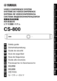 Yamaha CS 800
Manual
Yamaha CS 800
Manual
 Yamaha NS F210BL
User Manual
Yamaha NS F210BL
User Manual
 Yamaha ATS C300
User Manual
Yamaha ATS C300
User Manual
 Yamaha PASC9
User Manual
Yamaha PASC9
User Manual