Hisense 100L10E - Manuals
Hisense 100L10E – User Manual in PDF format online.
Manuals:
User Manual Hisense 100L10E


Summary
- 3 - Contents Contents ....................................................................................................................................................................... - 3 - Service Manual ........................................................................................
- 4 - Service Manual 1. Precautions and notices BEFORE SERVICING THE LCD TV, READ THE SAFETY PRECAUTIONS IN THIS MANUAL. USE ONLY MANUFACTURER SPECIFIED REPLACEMENT PARTS WHEN SERVICING. USE OF NON-AUTHORIZED PARTS WILL VOID THE MANUFACTURE'S WARRANTY Proper service and repair is important to the sa...
- 8 - • At all times other than when adjusting and checking the product, be sure to turn OFF the POWER Button and disconnect the power cable from the power source of the TV during servicing. • To prevent electric shock and breakage of PC board, start the servicing work at least 30 seconds after the ...
Hisense Manuals
-
 Hisense PX3 PRO
Installation Manual
Hisense PX3 PRO
Installation Manual
-
Hisense PX3 PRO
Manual
-
 Hisense AEH W41H1
User Manual
Hisense AEH W41H1
User Manual
-
 Hisense HRCD640TBW
User Manual
Hisense HRCD640TBW
User Manual
-
 Hisense HRCD640TS
User Manual
Hisense HRCD640TS
User Manual
-
Hisense HRCD640TSW
User Manual
-
 Hisense HT007E
User Manual
Hisense HT007E
User Manual
-
 Hisense HS205G
User Manual
Hisense HS205G
User Manual
-
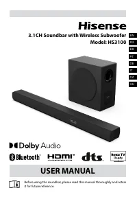 Hisense HS3100
User Manual
Hisense HS3100
User Manual
-
 Hisense HS5100
User Manual
Hisense HS5100
User Manual
-
 Hisense HRSBS540BW
User Manual
Hisense HRSBS540BW
User Manual
-
 Hisense 55A6N
User Manual
Hisense 55A6N
User Manual
-
 Hisense 75A6N
User Manual
Hisense 75A6N
User Manual
-
Hisense 75A6N
Installation Manual
-
Hisense 75A6N
Manual
-
 Hisense HSAA16FS
Manual
Hisense HSAA16FS
Manual
-
 Hisense HSAP16FB
Manual
Hisense HSAP16FB
Manual
-
Hisense WD16 E720XI
Manual
-
Hisense WD16 E722BXI
Manual
-
 Hisense 50U6HF
User Manual
Hisense 50U6HF
User Manual