Micron 2933 - User Manual
Micron 2933 RAM & Storage – User Manual, read for free online in PDF format. We hope this helps you resolve any issues you may have. If you have further questions, please contact us through the contact form.
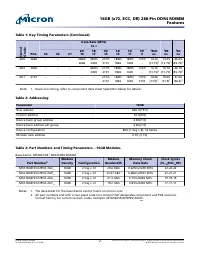
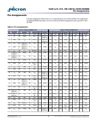
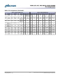
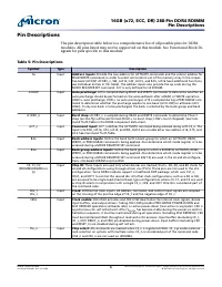
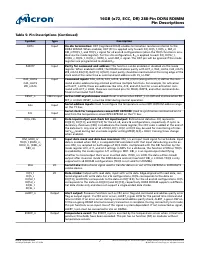
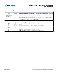
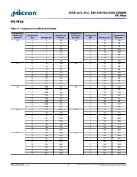
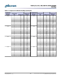
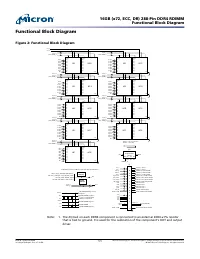
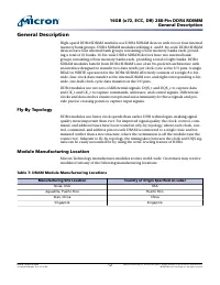
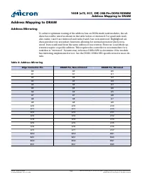
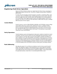
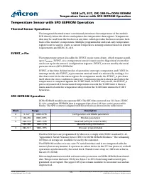
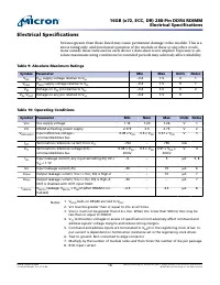
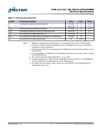
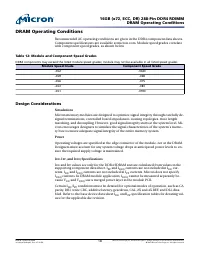
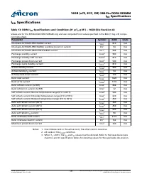

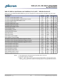
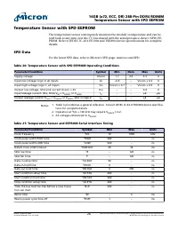
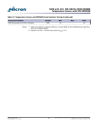
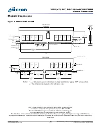
Table of Contents:
- Page 2 – Table 3: Part Numbers and Timing Parameters – 16GB Modules; Features
- Page 3 – Automotive Applications.; Important Notes and Warnings
- Page 4 – Table 4: Pin Assignments; Pin Assignments
- Page 6 – Table 5: Pin Descriptions; Pin Descriptions
- Page 9 – DQ Map
- Page 11 – Figure 2: Functional Block Diagram; Functional Block Diagram
- Page 12 – Module Manufacturing Location; Table 7: DRAM Module Manufacturing Locations; Manufacturing Site Location; General Description
- Page 13 – Address Mirroring; Table 8: Address Mirroring; Edge Connector Pin; Address Mapping to DRAM
- Page 14 – Registering Clock Driver Operation; Control Words; C bus interface resides on the same I; Parity Operations
- Page 15 – Thermal Sensor Operations; SPD EEPROM Operation; Block; The EEPROM resides on a two-wire I; Temperature Sensor with SPD EEPROM Operation
- Page 16 – Table 9: Absolute Maximum Ratings; Electrical Specifications
- Page 17 – Table 11: Thermal Characteristics
- Page 18 – Table 12: Module and Component Speed Grades; Module Speed Grade; Design Considerations; Simulations; Specifications; DRAM Operating Conditions
- Page 19 – Specifications and Conditions (0°; Parameter
- Page 25 – Table 19: Registering Clock Driver Electrical Characteristics; Registering Clock Driver Specifications
- Page 26 – SPD Data; Table 21: Temperature Sensor and EEPROM Serial Interface Timing; Temperature Sensor with SPD EEPROM
- Page 28 – Front view; The dimensional diagram is for reference only.; Module Dimensions
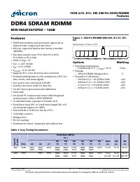
DDR4 SDRAM RDIMM
MTA18ASF2G72PDZ – 16GB
Features
• DDR4 functionality and operations supported as
defined in the component data sheet
• 288-pin, registered dual in-line memory module
(RDIMM)
• Fast data transfer rates: PC4-3200, PC4-2933,
PC4-2666, or PC4-2400
• 16GB (2 Gig × 72)
• V
DD
= 1.20V (NOM)
• V
PP
= 2.5V (NOM)
• V
DDSPD
= 2.5V (NOM)
• Supports ECC error detection and correction
• Nominal and dynamic on-die termination (ODT) for
data, strobe, and mask signals
• Low-power auto self refresh (LPASR)
• Data bus inversion (DBI) for data bus
• On-die V
REFDQ
generation and calibration
• Dual-rank
• On-board I
2
C temperature sensor with integrated
serial presence-detect (SPD) EEPROM
• 16 internal banks; 4 groups of 4 banks each
• Fixed burst chop (BC) of 4 and burst length (BL) of 8
via the mode register set (MRS)
• Selectable BC4 or BL8 on-the-fly (OTF)
• Gold edge contacts
• Halogen-free
• Fly-by topology
• Terminated control, command, and address bus
Figure 1: 288-Pin RDIMM (MO-309, R/C-E1, R/C-
E2)
Module height: 31.25mm (1.23in)
Options
Marking
• Operating temperature
– Commercial (0°C
≤
T
OPER
≤
95°C)
None
• Package
– 288-pin DIMM (halogen-free)
Z
• Frequency/CAS latency
– 0.625ns @ CL = 22 (DDR4-3200)
-3G2
– 0.682ns @ CL = 21 (DDR4-2933)
-2G9
– 0.75ns @ CL = 19 (DDR4-2666)
-2G6
– 0.83ns @ CL = 17 (DDR4-2400)
-2G3
Table 1: Key Timing Parameters
Speed
Grade
PC4-
Data Rate (MT/s)
CL =
t
RCD
ns
t
RP
ns
t
RC
ns
24
22
21
20\
19
18\
17
16\
15
14\
13
12\
11
10\
9
-3G2
3200
3200,
2933
3200,
2933
2933
2666\
2666
2400\
2400
2133\
2133
1866\
1866
1600\
1600
1333\
–
13.75
13.75
45.75
-2G9
2933
–
2933
2933
2666\
2666
2400\
2400
2133\
2133
1866\
1866
1600\
1600
1333\
–
14.32
14.32
(13.75)
46.32
(45.75)
16GB (x72, ECC, DR) 288-Pin DDR4 RDIMM
Features
CCMTD-1725822587-9899
asf18c2gx72pdz.pdf - Rev. H 7/19 EN
1
Micron Technology, Inc. reserves the right to change products or specifications without notice.
© 2015 Micron Technology, Inc. All rights reserved.
Products and specifications discussed herein are subject to change by Micron without notice.
"Loading the manual" means you need to wait until the file loads and becomes available for online reading. Some manuals are very large, and the time they take to appear depends on your internet speed.
Summary
Table 1: Key Timing Parameters (Continued) Speed Grade PC4- Data Rate (MT/s) CL = t RCD ns t RP ns t RC ns 24 22 21 20\ 19 18\ 17 16\ 15 14\ 13 12\ 11 10\ 9 -2G6 2666 – – – 2666\ 2666 2400\ 2400 2133\ 2133 1866\ 1866 1600\ 1600 1333\ – 14.25 (13.75) 1 14.25 (13.75) 1 46.25 (45.75) 1 -2G3 2400 – – – ...
Important Notes and Warnings Micron Technology, Inc. ("Micron") reserves the right to make changes to information published in this document,including without limitation specifications and product descriptions. This document supersedes and replaces allinformation supplied prior to the public...
Pin Assignments The pin assignment table below is a comprehensive list of all possible pin assignmentsfor DDR4 RDIMM modules. See the Functional Block Diagram for pins specific to thismodule. Table 4: Pin Assignments 288-Pin DDR4 RDIMM Front 288-Pin DDR4 RDIMM Back Pin Symbol Pin Symbol Pin Symbol P...