Page 2 - Table 3: Part Numbers and Timing Parameters – 16GB Modules; Features
Table 1: Key Timing Parameters (Continued) Speed Grade PC4- Data Rate (MT/s) CL = t RCD ns t RP ns t RC ns 24 22 21 20\ 19 18\ 17 16\ 15 14\ 13 12\ 11 10\ 9 -2G6 2666 – – – 2666\ 2666 2400\ 2400 2133\ 2133 1866\ 1866 1600\ 1600 1333\ – 14.25 (13.75) 1 14.25 (13.75) 1 46.25 (45.75) 1 -2G3 2400 – – – ...
Page 3 - Automotive Applications.; Important Notes and Warnings
Important Notes and Warnings Micron Technology, Inc. ("Micron") reserves the right to make changes to information published in this document,including without limitation specifications and product descriptions. This document supersedes and replaces allinformation supplied prior to the public...
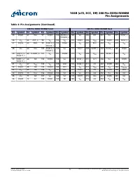
Page 4 - Table 4: Pin Assignments; Pin Assignments
Pin Assignments The pin assignment table below is a comprehensive list of all possible pin assignmentsfor DDR4 RDIMM modules. See the Functional Block Diagram for pins specific to thismodule. Table 4: Pin Assignments 288-Pin DDR4 RDIMM Front 288-Pin DDR4 RDIMM Back Pin Symbol Pin Symbol Pin Symbol P...
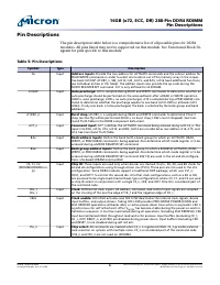
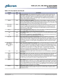
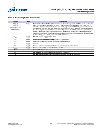
Page 6 - Table 5: Pin Descriptions; Pin Descriptions
Pin Descriptions The pin description table below is a comprehensive list of all possible pins for DDR4modules. All pins listed may not be supported on this module. See Functional Block Di-agram for pins specific to this module. Table 5: Pin Descriptions Symbol Type Description Ax Input Address input...
Page 9 - DQ Map
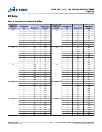
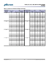
DQ Map Table 6: Component-to-Module DQ Map Component Reference Number Component DQ Module DQ Module Pin Number Component Reference Number Component DQ Module DQ Module Pin Number U2 0 3 157 U3 0 11 168 1 0 5 1 8 16 2 2 12 2 10 23 3 1 150 3 9 161 4 7 155 4 15 166 5 4 3 5 12 14 6 6 10 6 14 21 7 5 148 ...
Page 11 - Figure 2: Functional Block Diagram; Functional Block Diagram
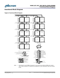
Functional Block Diagram Figure 2: Functional Block Diagram DQ DQ DQ DQ DQ DQ DQ DQ ZQ DQ0 DQ1 DQ2 DQ3 DQ4 DQ5 DQ6 DQ7 U2 DQ DQ DQ DQ DQ DQ DQ DQ U20 DQ32 DQ33 DQ34 DQ35 DQ36 DQ37 DQ38 DQ39 U8 DQ DQ DQ DQ DQ DQ DQ DQ U15 DQ8 DQ9 DQ10 DQ11 DQ12 DQ13 DQ14 DQ15 U3 DQ DQ DQ DQ DQ DQ DQ DQ U19 DQ40 DQ41 ...
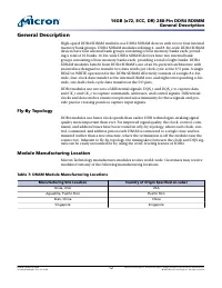
Page 12 - Module Manufacturing Location; Table 7: DRAM Module Manufacturing Locations; Manufacturing Site Location; General Description
General Description High-speed DDR4 SDRAM modules use DDR4 SDRAM devices with two or four internalmemory bank groups. DDR4 SDRAM modules utilizing 4- and 8-bit-wide DDR4 SDRAMdevices have four internal bank groups consisting of four memory banks each, provid-ing a total of 16 banks. 16-bit-wide DDR4...
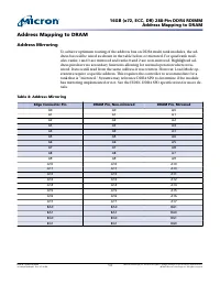
Page 13 - Address Mirroring; Table 8: Address Mirroring; Edge Connector Pin; Address Mapping to DRAM
Address Mapping to DRAM Address Mirroring To achieve optimum routing of the address bus on DDR4 multi rank modules, the ad-dress bus will be wired as shown in the table below, or mirrored. For quad rank mod-ules, ranks 1 and 3 are mirrored and ranks 0 and 2 are non-mirrored. Highlighted ad-dress pin...
Page 14 - Registering Clock Driver Operation; Control Words; C bus interface resides on the same I; Parity Operations
Registering Clock Driver Operation Registered DDR4 SDRAM modules use a registering clock driver device consisting of aregister and a phase-lock loop (PLL). The device complies with the JEDEC DDR4 RCDspecification. To reduce the electrical load on the host memory controller's command, address, andcon...
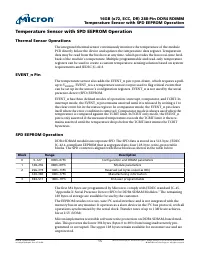
Page 15 - Thermal Sensor Operations; SPD EEPROM Operation; Block; The EEPROM resides on a two-wire I; Temperature Sensor with SPD EEPROM Operation
Temperature Sensor with SPD EEPROM Operation Thermal Sensor Operations The integrated thermal sensor continuously monitors the temperature of the modulePCB directly below the device and updates the temperature data register. Temperaturedata may be read from the bus host at any time, which provides t...
Page 16 - Table 9: Absolute Maximum Ratings; Electrical Specifications
Electrical Specifications Stresses greater than those listed may cause permanent damage to the module. This is astress rating only, and functional operation of the module at these or any other condi-tions outside those indicated in each device's data sheet is not implied. Exposure to ab-solute maxim...
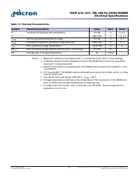
Page 17 - Table 11: Thermal Characteristics
Table 11: Thermal Characteristics Symbol Parameter/Condition Value Units Notes T C Commercial operating case temperature 0 to 85 °C 1, 2, 3 T C >85 to 95 °C 1, 2, 3, 4 T OPER Normal operating temperature range 0 to 85 °C 5, 7 T OPER Extended temperature operating range (optional) >85 to 95 °C ...
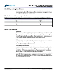
Page 18 - Table 12: Module and Component Speed Grades; Module Speed Grade; Design Considerations; Simulations; Specifications; DRAM Operating Conditions
DRAM Operating Conditions Recommended AC operating conditions are given in the DDR4 component data sheets.Component specifications are available at micron.com. Module speed grades correlatewith component speed grades, as shown below. Table 12: Module and Component Speed Grades DDR4 components may ex...
Page 19 - Specifications and Conditions (0°; Parameter
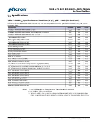
I DD Specifications Table 13: DDR4 I DD Specifications and Conditions (0° ≤ T C ≤ 85°) – 16GB (Die Revision A) Values are for the MT40A1G8 DDR4 SDRAM only and are computed from values specified in the 8Gb (1 Gig × 8) compo-nent data sheet. Parameter Symbol 2400 Units One bank ACTIVATE-PRECHARGE curr...
Page 25 - Table 19: Registering Clock Driver Electrical Characteristics; Registering Clock Driver Specifications
Registering Clock Driver Specifications Table 19: Registering Clock Driver Electrical Characteristics DDR4 RCD01 devices or equivalent Parameter Symbol Pins Min Nom Max Units DC supply voltage V DD – 1.14 1.2 1.26 V DC reference voltage V REF V REFCA 0.49 × V DD 0.5 × V DD 0.51 × V DD V DC terminati...
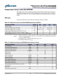
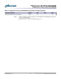
Page 26 - SPD Data; Table 21: Temperature Sensor and EEPROM Serial Interface Timing; Temperature Sensor with SPD EEPROM
Temperature Sensor with SPD EEPROM The temperature sensor continuously monitors the module's temperature and can beread back at any time over the I 2 C bus shared with the serial presence-detect (SPD) EE- PROM. Refer to JEDEC JC-42.4 EE1004 and TSE2004 device specifications for completedetails. SPD ...
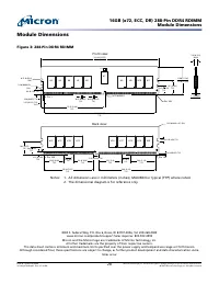
Page 28 - Front view; The dimensional diagram is for reference only.; Module Dimensions
Module Dimensions Figure 3: 288-Pin DDR4 RDIMM 31.40 (1.236)31.10 (1.224) 2.50 (0.098) D (2X) 0.75 (0.03) R (8X) Front view 133.48 (5.255)133.22 (5.244) Back view 1.5 (0.059)1.3 (0.051) 3.9 (0.153) MAX 3.0 (0.118) (4X) TYP 9.5 (0.374) TYP Pin 1 4.8 (0.189) TYP 5.95 (0.234) TYP 126.65 (4.99) TYP 0.85...