Casio CTK-711EX- Manuals
Casio CTK-711EX– User Manual in PDF format online.
Manuals:
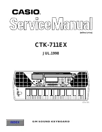
User Manual Casio CTK-711EX


Summary
— 1 — CONTENTS Safety Notice ----------------------------------------------------------------------------------------------- 2 Specifications ---------------------------------------------------------------------------------------------- 3 Important Operation -----------------------------------------...
— 2 — SAFETY NOTICE CAUTION!Danger of explosion if battery is incorrectly replaced. Replaceonly with the same or equivalent type. ADVARSE!Lithiumbatteri. Eksplosionsfare ved fejlagtig handtering.Udskiftning ma kun ske med batteri af samme fabrikat og type.Lever det brugte batteri tilbage tili levera...
— 3 — SPECIFICATIONS GENERAL Keyboard: 61 standard-size keys, 5 octaves (with touch response on/off; ExLight/Light/Normal/Heavy touch) Tones: 232 (128 General MIDI, 64 variation, 8 drum, 32 user); with layer andsplit Rhythm instrument tones: 53 Polyphony: 32 notes maximum (16 for certain tones) Digi...
Casio Manuals
-
 Casio 0205-H
User Manual
Casio 0205-H
User Manual
-
Casio 0205-H
Manual
-
 Casio 1174
User Manual
Casio 1174
User Manual
-
Casio 1174
Manual
-
 Casio 120CR
User Manual
Casio 120CR
User Manual
-
Casio 120CR
Manual
-
 Casio 120CR, 160CR
User Manual
Casio 120CR, 160CR
User Manual
-
 Casio 120ER
User Manual
Casio 120ER
User Manual
-
 Casio 130CR
User Manual
Casio 130CR
User Manual
-
Casio 130CR
Manual
-
 Casio 140CR
Manual
Casio 140CR
Manual
-
 Casio 160CR
User Manual
Casio 160CR
User Manual
-
Casio 160CR
Manual
-
 Casio 1633
User Manual
Casio 1633
User Manual
-
Casio 1633
Manual
-
 Casio Модуль 1789
User Manual
Casio Модуль 1789
User Manual
-
 Casio 1868
User Manual
Casio 1868
User Manual
-
Casio 1868
Manual
-
 Casio 1949
User Manual
Casio 1949
User Manual
-
Casio 1949
Manual